Treasury
3-MO 3.91% +2bp 6-MO 3.98% +3bp 1-YR 4.13% +2bp 2-YR 4.37% +3bp 3-YR 4.45% +4bp 5-YR 4.54% +2bp 7-YR 4.65% +2bp 10-YR 4.78% +1bp 20-YR 5.25% unch 30-YR 5.24% -1bp 3-MO 3.91% +2bp 6-MO 3.98% +3bp 1-YR 4.13% +2bp 2-YR 4.37% +3bp 3-YR 4.45% +4bp 5-YR 4.54% +2bp 7-YR 4.65% +2bp 10-YR 4.78% +1bp 20-YR 5.25% unch 30-YR 5.24% -1bp 3-MO 3.91% +2bp 6-MO 3.98% +3bp 1-YR 4.13% +2bp 2-YR 4.37% +3bp 3-YR 4.45% +4bp 5-YR 4.54% +2bp 7-YR 4.65% +2bp 10-YR 4.78% +1bp 20-YR 5.25% unch 30-YR 5.24% -1bp 3-MO 3.91% +2bp 6-MO 3.98% +3bp 1-YR 4.13% +2bp 2-YR 4.37% +3bp 3-YR 4.45% +4bp 5-YR 4.54% +2bp 7-YR 4.65% +2bp 10-YR 4.78% +1bp 20-YR 5.25% unch 30-YR 5.24% -1bp 3-MO 3.91% +2bp 6-MO 3.98% +3bp 1-YR 4.13% +2bp 2-YR 4.37% +3bp 3-YR 4.45% +4bp 5-YR 4.54% +2bp 7-YR 4.65% +2bp 10-YR 4.78% +1bp 20-YR 5.25% unch 30-YR 5.24% -1bp 3-MO 3.91% +2bp 6-MO 3.98% +3bp 1-YR 4.13% +2bp 2-YR 4.37% +3bp 3-YR 4.45% +4bp 5-YR 4.54% +2bp 7-YR 4.65% +2bp 10-YR 4.78% +1bp 20-YR 5.25% unch 30-YR 5.24% -1bp
US Treasury par yield curve · Sep 4 · Source: U.S. Treasury
Tuesday, September 8, 2026
U.S. Edition
Chipmaking

ASML and TSMC target a 12-inch photomask pilot line by 2031
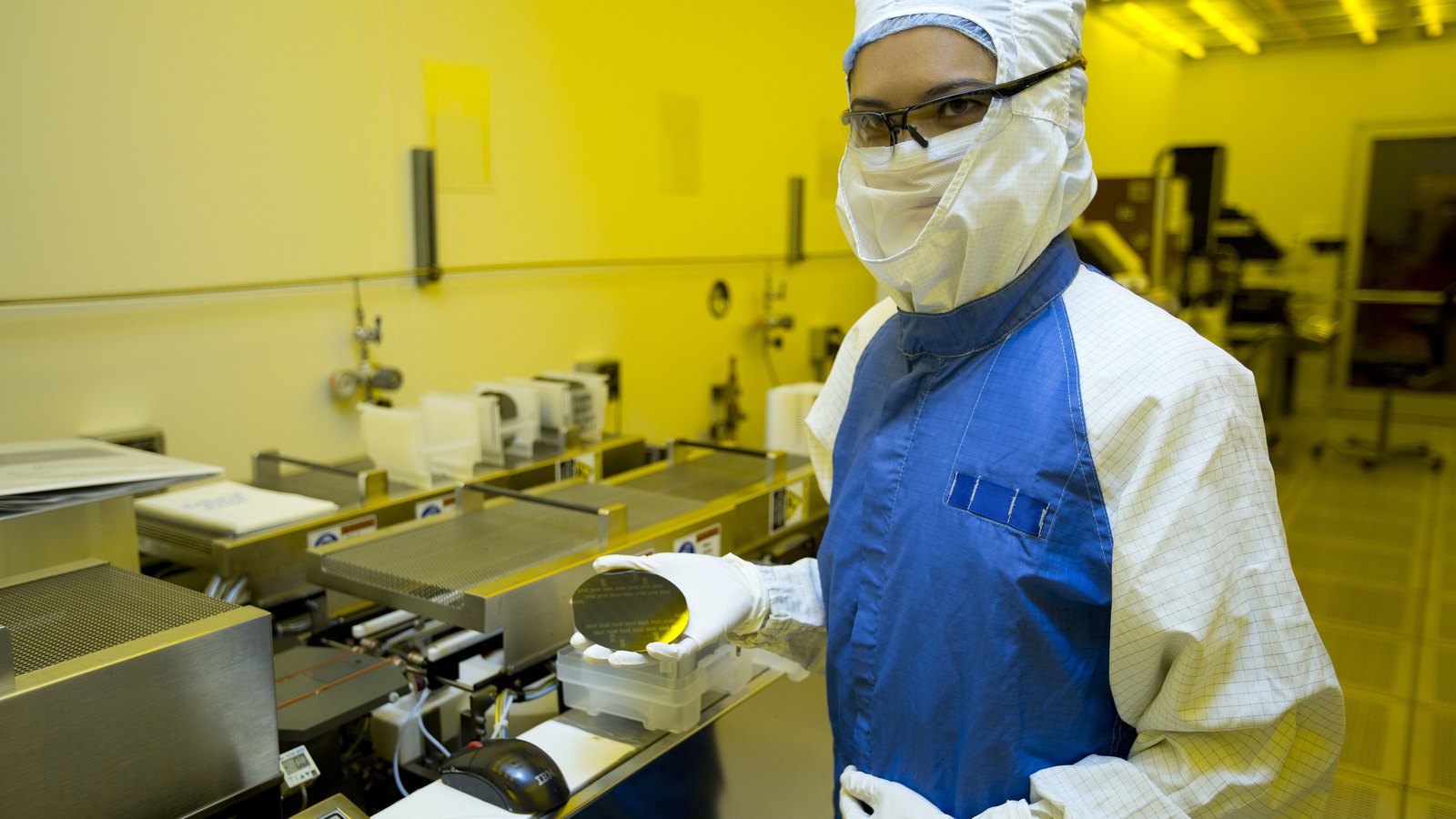
A semiconductor cleanroom worker holds a silicon wafer beside processing equipment
Photo: U.S. Department of Energy / Wikimedia Commons (Public domain)

The mask would double in width.

ASML and TSMC have started an industry initiative to move High NA extreme-ultraviolet lithography from 6-inch to 12-inch photomasks, the companies said Tuesday. They target a pilot line in 2031 and production readiness for advanced chips in 2033.

TSMC separately intends to begin high-volume manufacturing with High NA EUV in 2030, using the established 6-inch format first.

The larger masks are meant to improve scanner productivity, lower costs and remove constraints from joining multiple mask patterns. Those are targets. No 12-inch production capacity exists in the announcement, and the companies did not disclose a project cost.